半导体/集成电路

  • 晶圆和半导体工业测量-capa

    晶圆和半导体工业测量-capa

    半导体工业当中,为了实现工艺要求和生产效率,需要满足超高精度的测量。德国米铱公司提供的电容式位移传感器被用于以纳米级的精度校准芯片光刻机中镜片的位置,测量晶圆厚度等应用。Extreme accuracies are required in the semiconductor industry in order to design processes and products efficiently. Capacitive sensors from Micro-Epsilon are used, among other things, for the positioning, displacement measurement and thickness measurement in the semiconductors area. 以纳米级的精度校准芯片光刻机中镜片的位置 晶圆厚度三点测[详细]
  • 硅锭外型检测-2D/3D

    硅锭外型检测-2D/3D

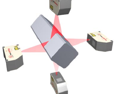
    本案例用于测量多晶硅锭的众多属性,如边长,角度或者对角线长度。硅锭的表面光洁度也可以得到测量。采用激光轮廓扫描仪的好处很多,如非接触,免磨损以及对被测物体无机械影响。相对于人工检测,该系统稳定性非常高。The optical dimensionCONTROL 8260 for Ingots inspection system for silicon ingots automatically measures the surface of the ingot and automatically performs, among other things, a measurement of the side lengths, phase lengths, angles and diagonal lengths. The flatness of the side surfaces is also [详细]
  • 电容生产中液位检测-confocal

    电容生产中液位检测-confocal

    在电容生产过程中,电容原件需要浸泡在特定液体内。为了确保浸泡过程遵守规格要求,精确控制液位高度至关重要。传统测量采用激光三角反射式传感器存在许多固有问题,例如复杂的系统安装和调试,以及由此带来的费用升高。液面的波动还会带来信号的中断。光谱共焦式传感器可以解决上述问题。通过光谱共焦原理,溶剂表面的反射光被直接测量。液面的蒸汽产生的干扰也可以通过特殊处理得以解决。During the production process capacitor elements must be dipped in a defined manner into a bath of liquid. To ensure constantly high quality it is crucialthat the capacitor elements are dipped exactly according to the s[详细]
  • 集成电路管脚整体平整度检测-opto

    集成电路管脚整体平整度检测-opto

    集成电路芯片管脚在插入印刷电路板后,需要检测管脚是否全部就位,之后才会进入焊接流程。芯片管脚就位的整体平整度对电路板焊接质量至关重要。在最先进的贴片机中,元器件的整体平整度可以通过激光三角反射式位移传感器进行实时在线检测。The term ?co-planarity“ describes theproper seating of the tips of fine-pitch device leads on the copper pads on aPCB prior to solder process. The co-planarity is a critical dimension for thequality of the soldered joints, because no reliable and correct soldering canbe done if there is a[详细]

版权所有:米铱(北京)测试技术有限公司 服务热线:010-64398534  京ICP备14053538号

在线留言 相关资讯 技术支持: 神州宏网

京公网安备 11011302002621号